Charlieplexing reloaded von Gerd Sinning
Ein
etwas älteres Projekt war mal ein Thermometer mit 12 Leds in einer
Reihe, mit dem AT15 und Charlieplexing. Das habe ich nochmal gebaut mit
dem AT13, aber das Programm sollte jetzt Basic sein. Das erste war
Cplex0.bas, zum Test der Verdrahtung empfehlenswert. Das funktioniert.
Dann kam Cplex3.bas mit dem ADC2 an PB4. Das funktioniert nicht, der
ADC liefert keine eindeutigen Daten. Merkwürdig. Nun hatte ich schon
das Assembler Programm für den AT15, das habe ich dann für den AT13
umgeschrieben. Siehe da, das funktioniert wie es soll, die Spannung am
ADC steuert eine Led an. Die Verdrahtung ist wie bei der Cplex Clock,
nur in einer Reihe. Die thresholds für die Spannung liegen in einer
Tabelle, das ist flexibel, hier sind sie linear angeordnet, aber für
ein VU-meter geht es auch logarithmisch. Warum geht's mit Basic nicht,
mein Programm ist V 1.11.9.8, also schon älter, vielleicht liegt es
daran.
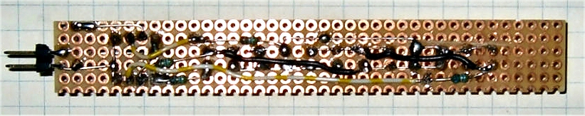
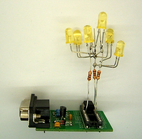
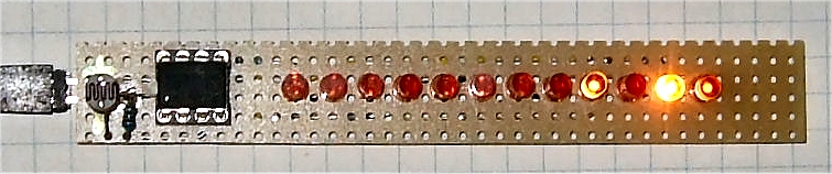
Die
Bilder zeigen den Aufbau für Cplex1T.asm. Mit einem LDR an + und 68 k
an Gnd und die Mitte an PB4 hat man ein Miniluxmeter. Der LDR ist ja
schon logarithmisch, das passt dann. Kann man an die Wand hängen.
Download:
Cplexe.zip'***************************************************************************
'
'ATTiny13 12 Charlieplexed Leds on PB 0 1 2 3
'
'
' input on ADC channel 2
'
'***************************************************************************
' This program is free software; you can redistribute it and/or
' modify it under the terms of the GNU General Public License.
' This program is distributed in the hope that it will be useful,
' but WITHOUT ANY WARRANTY;
'
'***************************************************************************
'
' Pinout ATtiny13/ATtiny13V 8-PDIP/SOIC
'
' (PCINT5/RESET/ADC0/dW) PB5 VCC
' (PCINT3/CLKI/ADC3) PB3 PB2 (SCK/ADC1/T0/PCINT2)
' (PCINT4/ADC2) PB4 PB1 (MISO/AIN1/OC0B/INT0/PCINT1)
' GND PB0 (MOSI/AIN0/OC0A/PCINT0)
'
'***************************************************************************
' PB0 output Led
' PB1 output
' PB2 output
' PB3 output
' PB4 input ADC channel 2
'***************************************************************************
$regfile = "attiny13.dat"
$crystal = 1200000
$hwstack = 8
$swstack = 8
$framesize = 4
Const C_value = 187 - 1 ' Compare Match IRQ 10 ms
Declare Sub Mydelay
Dim Voltage As Word , Avgv As Word
Dim Icnt0 As Byte
Dim N As Byte , Xp As Byte , Xd As Byte
'Dim Pp As Byte , Dd As Byte
Portb = &B00000000
Ddrb = &B00000000
Acsr.acd = 1 ' switch off analog comparator
Config Adc = Single , Prescaler = Auto , Reference = Avcc
Didr0.adc2d = 1
Start Adc
Config Timer0 = Timer , Prescale = 64
Ocr0a = C_value ' value for 1.2 MHz
Tccr0a = &B00000010 ' ctc
Timsk0.ocie0a = 1
On Oc0a Tim0_compa
Start Timer0
For N = 0 To 11 'test leds
Xd = Lookup(n , Led12)
Xp = Xd
Shift Xd , Right , 4 ' upper is DDR
Xd = Xd And &H0F
Xp = Xp And &H0F ' lower is Port
Portb = Xp
Ddrb = Xd
Call Mydelay
Next N
Enable Interrupts
Timer0 = 0
Do ' main loop
Loop
'***************************************************************************
'Tim0_compa Interrupt 10 ms
'***************************************************************************
Tim0_compa: '
'Incr Icnt0
Voltage = Getadc(2)
Avgv = Getadc(2)
Voltage = Avgv + Voltage
N = Voltage / 170
If N = 12 Then
N = 11
End If
Xd = Lookup(n , Led12)
Xp = Xd
Shift Xd , Right , 4 ' upper is DDR
Xd = Xd And &H0F
Xp = Xp And &H0F ' lower is Port
Portb = Xp
Ddrb = Xd
'Voltage = Getadc(2)
'Avgv = Avgv + Voltage
'Shift Voltage , Right , 2 '8 bit
Return
End
Mydelay: 'delay
$asm
PUSH R27
Ldi R27 , 200 'Load R27
Mdec:
Dec R27
BRNE Mdec
POP R27
$end Asm
Return
Led12: ' Led0..11 Cplex ' 12 = 0 upper 4 bit DDRB lower 4 bit PORTB
Data &B00110001 , &B11001000 , &B11000100 , &B10101000 , &B10100010 , &B01100100 , &B01100010 , &B01010100 , &B01010001 , &B10011000 , &B10010001 , &B00110010 , 0 , 0
Assembler-Version:
;***************************************************************************
; ATtiny13 Charlieplex 12 Leds on PB 0 1 2 3, use threshold and Led table
;
; input on ADC2, PB4, 8 bit
; simple Voltmeter, 0,..,5 V, single Led is on
; bsed on ATtiny15 GS 2009
; The timing is adapted for 1.2 MHz
;
;***************************************************************************
; This program is free software; you can redistribute it and/or
; modify it under the terms of the GNU General Public License.
; This program is distributed in the hope that it will be useful,
; but WITHOUT ANY WARRANTY;
;
;***************************************************************************
; Pinout ATtiny13/ATtiny13V 8-PDIP/SOIC
;
; (PCINT5/RESET/ADC0/dW) PB5 VCC
; (PCINT3/CLKI/ADC3) PB3 PB2 (SCK/ADC1/T0/PCINT2)
; (PCINT4/ADC2) PB4 PB1 (MISO/AIN1/OC0B/INT0/PCINT1)
; GND PB0 (MOSI/AIN0/OC0A/PCINT0)
;***************************************************************************
; PB4 input ADC2
; PB3 output Leds
; PB2 output
; PB1 output
; PB0 output
;***************************************************************************
.DEVICE ATtiny13 ;for gavrasm
.equ avgcnt = 16
.equ AD_resolution = 256 ; A/D converter resolution
; r0 used
.def S = r4
.def temp = r16
.def count = r17
.def lcnt = r18
.def next_step = r19
.def av_l = r20 ; Average Low Byte (ADC Measurement)
.def av_h = r21 ; Average High Byte (ADC Measurement)
.def LedPD = R22 ; Led port and DDR
.def Ledcnt = R23 ; Led 0,..,11
.def ZL = r30
.def ZH = r31
.cseg
.org 0
rjmp reset ; 0x0000 Reset-vector
reti ; 0x0001 External Interrupt 0
reti ; 0x0002 PCIrq0
rjmp TIM0_OVF ; 0x0003 Timer/Counter0 Overflow
reti
;********************************************************************
;* "TIM0_OVF" - Timer/counter overflow interrupt handler
;*
;* The overflow interrupt fires every 1.7ms
;*
;********************************************************************
TIM0_OVF: in S,sreg ; Updated every 1.7 ms, calibrate OSCCAL
inc count
inc next_step
out sreg,S
reti
;***************************************************************************
reset:
; writing calibration byte to OSCCAL Register.
;ldi temp,0x7F ; test
;out OSCCAL,temp ; for the clock
nop
nop
; Port B
ldi temp,0 ; set
out PORTB, temp ; 1 = pull-up , 0 = float
ldi temp,0 ; 1 = output , 0 = input
out DDRB, temp ; to data direction register
;***************************************************************************
; AD-Converter setup:
; If ADLAR is set, the result is left-adjusted.
ldi temp, 0b00100010 ; Ch 2 input=PB4, REFS0,1 =00 Vcc is RefVoltage
out ADMUX, temp
; ADC init single conversion prescaler 8:
ldi temp, 0b11010011 ;
out ADCSRA, temp
;***************************************************************************
; timer setup:
ldi temp,0b00000010 ; Timer/Counter 0 clocked at CK/8
out TCCR0B,temp ; 1,2 Mhz
;Bit 1 – TOIE0: Timer/Counter0 Overflow Interrupt Enable
ldi temp,0b00000010 ; set Bit 1
out TIMSK0,temp ; in the Timer Interupt Mask Register
out TIFR0,temp ; in the Timer Interupt Flag Register
ldi temp,0 ; Timer/Counter 0 clear
out TCNT0,temp ;
clr av_l
clr av_h ; Clear Average Registers
clr next_step
sei ; Enable gobal iterrupt
;***************************************************************************
clr Ledcnt
ldi ZH,high(2*Led12) ; setup Z pointer hi
testleds:
ldi ZL,low(2*Led12) ; Leds upper 4 bit DDRB lower 4 bit PORTB
add ZL, Ledcnt ; table offset
lpm
tst r0 ; 0 is end of table
breq ma1
rcall Ledset ; set PORTB and DDRB
inc Ledcnt
clr next_step
testwait: cpi next_step, 250 ; wait time
brlo testwait
rjmp testleds
ma1: clr next_step
main: cpi next_step, 8 ; reaction time
brlo main
clr next_step
rcall convert_average ; Measure Volt 0..255
mc0:
ldi ZH, high(2*Thresh) ; setup Threshold
ldi ZL, low(2*Thresh) ; setup Z pointer lo
ser Ledcnt ; to -1
mc1:
lpm
tst r0
breq mc2
inc ZL
inc Ledcnt ; 0..11
cp av_l, r0 ; av higher than threshold
brsh mc1 ; else led on
mc2:
ldi ZH,high(2*Led12) ; setup Z pointer hi to Leds
ldi ZL,low(2*Led12) ; Leds upper 4 bit DDRB lower 4 bit PORTB
add ZL, Ledcnt ; table offset
lpm
rcall Ledset ; set PORTB and DDRB
rjmp main
;***************************************************************************
Ledset:
mov LedPD, r0 ; subroutine to set Leds, input r0
andi LedPD, 0x0F ; lower 4 bit PORTB
out PORTB, LedPD ; first Port
mov LedPD, r0
swap LedPD ; swap
andi LedPD, 0x0F ; upper 4 bit DDRB
out DDRB, LedPD ; to data direction register
ret
;*************************[ ADC Handler ]*********************************
; This function measures the ADC channel, and returns the
; converted value in [av_l] 8 bit resolution
convert_average:
ldi temp,0b00100010
out ADMUX, temp ; Set ADC Channel PB4
clr av_l
clr av_h ; Clear Average Registers
ldi lcnt,avgcnt ; Set loop counter
convert_start:
ldi temp,0b11010011 ;
out ADCSRA,temp ; Start A/D Conversions
convert_wait:
sbis ADCSRA, ADIF
rjmp convert_wait ; Wait for Conversion to finish
in temp, ADCH
add av_l, temp
ldi temp, 0
adc av_h, temp ; Add measured value to average
dec lcnt
brne convert_start ; Repeat lcnt times
ldi lcnt,avgcnt/4 ; Set shift counter
convert_avg:
lsr av_h
ror av_l ; av_h:av_l = av_h:av_l/2
dec lcnt
brne convert_avg ; Repeat (avg_loop_cnt) times
;cbi ADCSRA,ADEN
ret ; return to measure
;***************************************************************************
; force table to begin at 256 byte boundary
.org 0x100
; Charlieplex Leds on PB 0 1 2 3
; in 1 byte: upper 4 bit DDRB lower 4 bit PORTB
Led12: ;led0..11 Cplex
.db 0b00110001, 0b00110010,
.db 0b10010001, 0b10011000,
.db 0b01010001, 0b01010100,
.db 0b01100010, 0b01100100,
.db 0b10100010, 0b10101000,
.db 0b11000100, 0b11001000,
.db 0,0
; linear voltage threshold for Leds
Thresh:
.db 21, 42, 63, 85, 106, 127, 148, 170, 191, 210, 233, 255, 0, 0
Led6:
.db 0b10110001, 0b10110010,
.db 0b11100010, 0b11100100,
.db 0b11010100, 0b11010001,
.db 0,0
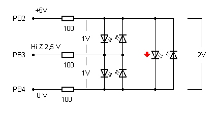
 Sechs LEDs an drei
Ports
Sechs LEDs an drei
Ports