 Dice with ATtiny15/13 Dice with ATtiny15/13
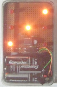
You may remember the times when families were sitting at a table rolling dice and using a game board to play. This one is the electronic version of a dice for modern kids. It won't roll off the table. Let's get ready to roll.
The start button will wake up the controller from sleep mode and the center led lights up to show the button is pressed. The program then counts the time while the start button is pressed and calculates a random roll time. When the button is released the dice start rolling, fast at first then slower and then stop to show the result. If the start button is not pressed then after about 10 seconds it goes to sleep mode again and the leds turn off. No on-off switch is needed here, it draws only few microamps in sleep mode.
It can be done easily with a few parts only : the AT15 controller, a switch, some resistors and 7 leds.
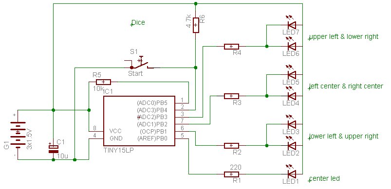
Schematic diagram
The center led is connected to PB0, the other leds are wired in parallel to the other ports, it needs only 4 output ports to display all possible combinations of a dice. For example to show a 3 the lower left and upper right leds and the center led are turned on. The start button is on PB4 and a Pin change Interrupt wakes up the AT15 from sleep mode.
How random will it be? It looks good to me but an improvement would be using a digital pseudorandom noise generator (described elsewhere) to generate the result displayed. To keep it simple the start button press down time is counted. Unlikely to get the same time twice, let's call it random for now.
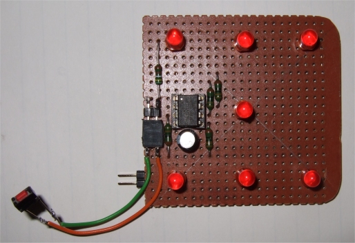
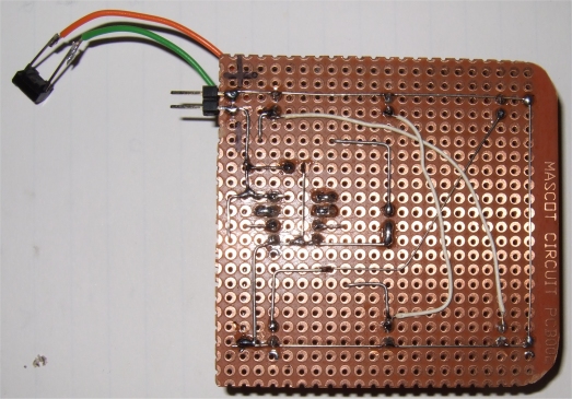
Front and back view of the circuit board
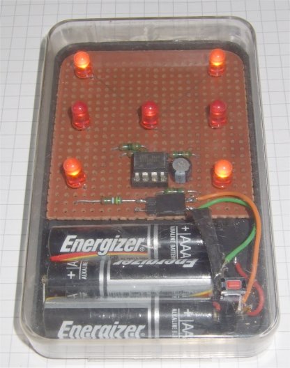
Dice in a box. When it's ready it has the size of a smartphone. If you can find a smartphone app, don't build it.
Download: DiceAsmHex.zipThis program is distributed in the hope that it will be useful but WITHOUT ANY WARRANTY;
References
Atmel datasheet ATtiny15 & ATtiny13, Atmel.com
Gerd's AVR assembler version 3.3: http://www.avr-asm-tutorial.net/gavrasm/index_en.html
Korrektur für Tiny13 ( PB3 und 4 waren vertauscht ): Dice13a.zip
;***************************************************************************
; AT13  rolling Dice
;	sleep mode ok, must turn off T/C0 first
;
;	connect + led - R to PBx, low is on
; 	based on ATtiny15 GS 12-2011
;	The timing was adapted for 1.6 MHz on AT15
;
;	changes AT15 -> AT13
;	Interrupt vectors, TCCR0->TCCR0B, TIMSK0, TIFR0, PCMSK
;	PB4->PB3
;
; The AT13 is shipped with CKSEL = “10”, SUT = “10”, and CKDIV8 programmed. The default
; clock source setting is therefore the Internal RC Oscillator running at 9.6 MHz with longest start-
; up time and an initial system clock prescaling of 8. -> 1.2MHz default
;
;***************************************************************************
;  This program is free software; you can redistribute it and/or
;  modify it under the terms of the GNU General Public License.
;  This program is distributed in the hope that it will be useful,
;  but WITHOUT ANY WARRANTY;
;
;***************************************************************************
;
;		Pinout ATtiny13/ATtiny13V   8-PDIP/SOIC
;
;(PCINT5/RESET/ADC0/dW)	PB5	VCC
;(PCINT3/CLKI/ADC3) 	PB3	PB2 (SCK/ADC1/T0/PCINT2)
;(PCINT4/ADC2) 		PB4	PB1 (MISO/AIN1/OC0B/INT0/PCINT1)
;			GND	PB0 (MOSI/AIN0/OC0A/PCINT0)
;
;***************************************************************************
;			ATtiny15 dip
;	(RESET/ADC0) 	PB5	VCC
;	(ADC3) 		PB4	PB2 (ADC1/SCK/T0/INT0)
;	(ADC2) 		PB3	PB1 (AIN1/MISO/OC1A)
;			GND	PB0 (AIN0/AREF/MOSI)
;
;***************************************************************************
; PB4	input  Inpin pushbutton
; PB3	output Dice3 upper left & lower right
; PB2	output Dice2 left center & right center
; PB1	output Dice1 lower left & upper right
; PB0	output Dice0 center led
;***************************************************************************

.DEVICE ATtiny13	;for gavrasm V3.3

;.equ	toggle		= PB0		; output toggle
.equ	Inpin		= PB3		; input	 pushbutton

.equ	reload		= 256 - 100	; 50 us x 100 = 5 ms Timer0
.equ	waittime	= 4		; wait x 5 ms Timer0
.equ	Ontime		= 1		; 1  seconds on
.equ	Offtime		= 10		;

.equ	Dice0		= PB0		; 1 center
.equ	Dice1		= PB1		; 2 ll ur
.equ	Dice2		= PB2		; 3 lc rc
.equ	Dice3		= PB4		; 4 ul lr

.def	S		= r14
.def	T0reload	= r15

.def	temp		= r16
.def 	countL		= r17	; main timing
.def	countSec	= r18
.def 	cntDice		= r19	; 0..5
.def	cntIn		= r20	; input

.def 	countdel	= r21
.def 	cntWait		= r22


.cseg
.org 0
; Reset-vector to adress 0000
	rjmp	reset
	reti 			; INT0addr= 0x0001 External Interrupt 0
	rjmp	PC_irq 		; PCI0addr= 0x0002 Pin change Interrupt
	rjmp	TIM0_OVF	; OVF0addr= 0x0003 Timer/Counter0 Overflow
	reti
	reti
	reti
	reti
	reti

;***************************************************************************
;* "TIM0_OVF" - Timer/counter0 overflow interrupt handler
;*
;* The overflow interrupt fires every 5 ms, more or less
;*
;***************************************************************************

TIM0_OVF:	in	S,sreg			; Updated every 5 ms, calibrate

		out	TCNT0,T0reload		; for 5 ms Interrupt

		;sbis	PINB, toggle		; skip if set
		;sbi	PORTB, toggle		; set output
		;sbic	PINB, toggle	 	; skip if set
		;cbi	PORTB, toggle

		inc	cntDice
		cpi	cntDice, 6		; 0..5
		brne	TIM0_1
		clr	cntDice

TIM0_1:
		inc	countL			; main timing
		cpi	CountL, 200		; 200 x 5 ms
		brne	TIM0_ex
		clr	countL			; every second
		inc	countSec		; seconds 0 to 255


TIM0_ex:	out	sreg,S
		reti

;***************************************************************************
;*		pin change interrupt
;***************************************************************************

PC_irq:		in	S,sreg

   		ldi      temp, (0<<SE)
   		out      MCUCR, temp
   		ldi      temp, (0<<PCIE)    	; disable pin change interrupts
   		out      GIMSK, temp

		ldi	temp,0b00001111 	; output, 1 = output , 0 = input
		out	DDRB,temp       	; to data direction register
		ldi	temp,0b00000011 	; Timer/Counter 0 clocked at CK/64 = 40 us
		out	TCCR0B,temp		; 1,6 Mhz
		out	sreg,S
		reti

;***************************************************************************
;*		Reset
;***************************************************************************

reset:
		; writing the calibration byte to the OSCCAL Register.
;		ldi	temp,0x70    		; test , config val
;		out	OSCCAL,temp 		; for the clock
		nop
		nop

		ldi	temp,0b00011111 	; set pullup
		out	PORTB,	temp		; 1 = pull-up , 0 = float
		ldi	temp,0b00001111 	; output, 1 = output , 0 = input
		out	DDRB,temp       	; to data direction register

;***************************************************************************

; timer0 setup:
		ldi	temp,0b00000010		; Bit 1 – TOIE0: Timer/Counter0 Overflow Interrupt Enable
		out	TIFR0,temp 		; clear pending Interrupt
		out	TIMSK0,temp 		; in the Timer Interupt Mask Register

		ldi	temp,0b00000011 	; Timer/Counter 0 clocked at CK/64 = 40 us
		out	TCCR0B,temp		; 1,6 Mhz
		ldi	temp, reload		; Timer/Counter 0 reload
		out	TCNT0,temp		; for 5 ms Interrupt

		mov	T0reload, temp

		sei				; Enable gobal interrupt


;***************************************************************************
; intro

		ldi	temp, 0b00001110
		out	PORTB,	temp		;
		clr	countL
I1:		cpi	countL, 100
		brlo	I1
		ldi	temp, 0b00001101
		out	PORTB,	temp		;
		clr	countL
I2:		cpi	countL, 100
		brlo	I2
		ldi	temp, 0b00001011
		out	PORTB,	temp		;
		clr	countL
I3:		cpi	countL, 100
		brlo	I3
		ldi	temp, 0b00000111
		out	PORTB,	temp		;
		clr	countL
I4:		cpi	countL, 100
		brlo	I4

		ldi	temp, 0b00001111
		out	PORTB,	temp		;

; main loop

loop:		sbis	PINB, Inpin		; skip if Inpin high
		rjmp	pinlo			; switch lo
pinhi:
		rjmp	loop			; no, loop

pinlo:
		clr	countdel
		rcall	Delay			; debounce
		sbic	PINB, Inpin		; skip if Inpin lo
		rjmp	loop			; else switch lo, go


		ldi	temp, 0b00001111	; all off when press btn
		out	PORTB,	temp		;
RndIn:						; try to make it a bit random
		inc 	cntIn			; count btn press time
		cbi	PORTB, Dice0		; show when pressed
		sbis	PINB, Inpin		; skip if Inpin high
		rjmp	RndIn
		sbi	PORTB, Dice0		; off

		clr	countL
		clr	countSec
		andi	cntIn, 0b00011111 	; random roll time
		sbr	cntIn, 0b00010000 	; 15..31

		ldi	cntWait, 25		; wait time

Show:
		rcall 	ShowDice
		clr	countL
S0:		cp	countL, cntWait
		brne	S0
		inc 	cntWait			; inc wait time
		inc 	cntWait
		dec	cntIn
		brne	Show

		clr	countL
		clr	countSec
waiton:
		cpi	countSec, Ontime	; wait Ontime 1 sec
		brlo	waiton


waitoff:
		cpi	countSec, Offtime	; wait Offtime 10 sec
		sbis	PINB, Inpin		; skip if Inpin hi
		rjmp	loop			; else switch lo, loop
		brlo	waitoff

off:		ldi	temp, 0b00001111
		out	PORTB,	temp		; all off
		ldi	temp, 0
		out	DDRB,temp       	; make input, data direction register
		out	TCCR0B,temp		; stop timer

   		ldi      temp, (1<<PCINT3)    	; mask pin change interrupts
   		out      PCMSK, temp		; on pin2
   		ldi      temp, (1<<PCIE)    	; Enable pin change interrupts
   		out      GIFR, temp		; clear flag
   		out      GIMSK, temp
		; Disable pullups, Enable sleep mode, Sleep => Power Down
   		ldi      temp, (1<<PUD |1<<SE | 1<<SM1 | 0<<SM0)
   		out      MCUCR, temp
   		sleep


		rjmp	loop			; loop


;***************************************************************************

Delay:
		dec	countdel
		brne	Delay
		ret


ShowDice:
		cpi	cntDice, 0		; 0..5	1
		brne	R1
		sbi	PORTB, Dice1
		sbi	PORTB, Dice2
		sbi	PORTB, Dice3
		cbi	PORTB, Dice0
		rjmp	Rx
R1:
		cpi	cntDice, 1		; 0..5	2
		brne	R2
		sbi	PORTB, Dice0
		sbi	PORTB, Dice2
		sbi	PORTB, Dice3
		cbi	PORTB, Dice1
		rjmp	Rx
R2:
		cpi	cntDice, 2		; 0..5	3
		brne	R3
		sbi	PORTB, Dice2
		sbi	PORTB, Dice3
		cbi	PORTB, Dice0
		cbi	PORTB, Dice1
		rjmp	Rx
R3:
		cpi	cntDice, 3		; 0..5	4
		brne	R4
		sbi	PORTB, Dice0
		sbi	PORTB, Dice2
		cbi	PORTB, Dice1
		cbi	PORTB, Dice3
		rjmp	Rx
R4:
		cpi	cntDice, 4		; 0..5	5
		brne	R5
		sbi	PORTB, Dice2
		cbi	PORTB, Dice0
		cbi	PORTB, Dice1
		cbi	PORTB, Dice3
		rjmp	Rx
R5:
		cpi	cntDice, 5		; 0..5	6
		brne	Rx
		sbi	PORTB, Dice0
		cbi	PORTB, Dice1
		cbi	PORTB, Dice2
		cbi	PORTB, Dice3
Rx:		ret