
Frequency Counter with 7segment display
This Frequency Counter is suitable to display the frequency of a frequency generator with an analog setting. It is a very simple counter and can be used as a module in a box with a frequency generator.
It does what it says, it measures frequencies up to 2 MHz and shows the frequency on a 6 digit 7 segment display. The resolution is 10 Hz, we have only 6 digits because I once got a bag full of 3 digit common anode displays and here we already use all available pins on an Atmel ATTiny2313. Here you see it in a box with two frequency generators and it shows the frequency in kHz.
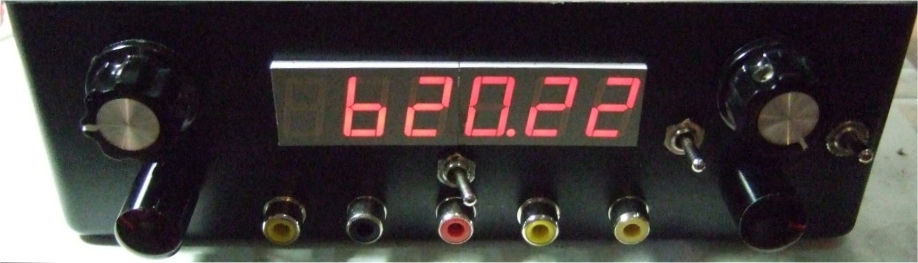
In the box, on the left is a 15Hz to 30 kHz dds sine wave generator and on the right is one with the famous XR2206, the switch below the display switches between the right and left side frequency display. Here it shows the maximum frequency of the XR2206.
Components needed for this small project are one Atmel ATTiny2313, eight 220 Ohm resistors, two 3 digit common anode displays and one 4 MHz quartz, which I just had in the box. It's possible to use e.g. a 8 MHz quartz which would extend the frequency to 4 MHz but then the the gate routines need adjustment, easy to do.
It is programmed in assembly language and compiled with gavrasm. Timer/Counter1 is used as the frequency counter and Timer/Counter0 for the gate time. At Timer/Counter1 count input T1 PD5 (Pin 9) the frequency is measured. A square wave should be present at this input so it could be wired to a Schmitt trigger front end as e.g. a 74HC132 to shape sinewaves.
With a prescaler of 64 and a compare value of 125 a Timer/Counter0 Compare Match A interrupt fires every 2 ms. This interrupt is used for for gate timing and to update the display. One software counter counts to 50, then stops Timer/Counter1 and displays the result. The gate time is 50 * 2 ms = 100 ms with a 4 MHz quartz. During this interrupt the display is updated. Leading zeros are blanked for easier reading and the decimal point is fixed in software.
The 7 seg digits are connected to PORTD, the segments to PORTB of
the 2313. Below are the details of one of the 3 digit common anode 7
seg display which I had available. You need to adjust if you have a
different display type.
 pin 12 11 10 09 08 07
    |-----------------|
    | d1 A  F d2 d3 B |  |--A--|
    |                 |  |F   B|
    |    top view     |  |--G--|
    |                 |  |E   C|
    | E  D dp C  G nc.|  |--D--|.dp
    |-----------------|
 pin 01 02 03 04 05 06

    2313 7 6 5 4 3 2 1  0  PORTB
    7seg 7 5 4 3 2 1 10 11 pin  12 9 8
    seg  B G C dp D E F A  dig   1 2 3 (3 = right dig)
                           PORTD 2 1 0
digit0 = PIND0, digit1 = PIND1, digit2 = PIND2, digit3 = PIND3, digit4 = PIND4, digit5 = PIND6
A standard perf board holds all components, the displays and some resistors
are wired vertically to give a small footprint of the assembly on the frontpanel.
All 7 seg pins are wired to the nearest port pin of the 2313, that is the easiest
way. It results in B G C dp D E F A for the segments and we need a translation
table to display the segments correctly. This is done in software, software
follows hardware as it should do. See translation table below.
Connections of the seven segment display cathodes:
number                           hex
   0| - f a b c d e | 01010000 | 50
   1| - - - b c - - | 01011111 | 5f
   2| g - a b - d e | 00110010 | 32
   3| g - a b c d - | 00010110 | 16
   4| g f - b c - - | 00011101 | 1d
   5| g f a - c d - | 10010100 | 94
   6| g f a - c d e | 10010001 | 91
   7| - - a b c - - | 01011110 | 5e
   8| g f a b c d e | 00010000 | 10
   9| g f a b c d - | 00011100 | 1c
   digit to seven segment LED mapping:
   seg B G C dp D E F A to portB 7..0
segments:
   0 1 2 3 4 5 6 7 8 9 blank
   .DB 0x50,0x5f,0x32,0x16,0x1d,0x94,0x91,0x5e,0x10,0x1c,0xFF,0x00
This is one way to build the frequency counter on a perf board, a quick project on a rainy weekend:
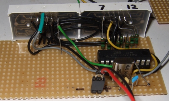
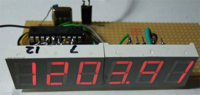
The top view of the counter, left is the wiring back view and front view on the right showing 1203.91 kHz
Finally the circuit diagram of the frequency counter:
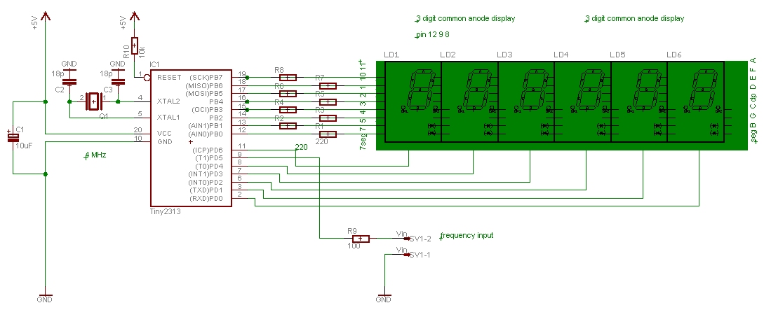
This frequency counter has only one option: measure frequency. As you can see all pins are used. Anyway I use it in my little frequency generator box and it works well.
This information and the program is distributed in the hope that it will be
useful but WITHOUT ANY WARRANTY;
download: 7segcnt4.asm
References
Gerd's AVR assembler version 2.7: http://www.avr-asm-tutorial.net/gavrasm/index_en.html
Induktivitätsmessung mit Zähler, von Gerd Sinning
Hier ist noch eine Idee zum L-Meter mit LM311. Das hat fast jeder mal gebaut. Ich habe das zusammen mit einem Frequenzzähler verwendet und die Daten in ein spreadsheat eingetragen und die Induktivität berechnet. Das geht gut wenn man gelegentlich damit arbeitet.
Der Frequenzzähler hat eine serielle Schnittstelle, und so habe ich dann ein PC Programm geschrieben, das die Frequenz auswertet und dann L anzeigt, digital und analog. Es ist recht einfach und rechnet mit double precision, aber es ist nur eine Idee für eigene Versuche.
;***************************************************************************
; Frequency counter 3, GS May-2010, ok
;
; Target ATiny2313
;
; Timer/Counter1 count input T1 PD5, Pin 9
; Timer/Counter0 Compare Match A, every 2 ms for gate timing
; gate time 100 ms, uses 4 MHz quartz
;
; uses 32 bit binary to packed BCD routines from Atmel application note
;
;  This program is free software; you can redistribute it and/or
;  modify it under the terms of the GNU General Public License.
;  This program is distributed in the hope that it will be useful,
;  but WITHOUT ANY WARRANTY;
;***************************************************************************
;
; 7 seg digits on PORTD, segments on PORTB
; uses 2 * 3 digit common anode 7 seg display, see below
;
;	pin	12 11 10 09 08 07
;	|------------------------------|
;	|	d1 A  F  d2 d3 B       |	|--A--|
;	|                              |	F     B
;	|	   top view            |	|--G--|
;       |                              |	E     C
;	|	E  D  dp C  G  nc.     |	|--D--|.dp
;	|------------------------------|
;	pin	01 02 03 04 05 06
;
; 2313 7  6  5  4  3  2  1  0    PORTB
; 7seg 7  5  4  3  2  1  10 11   pin 12 9 8
;  seg B  G  C dp  D  E  F  A    dig  1 2 3 (3 = right dig)
;                                 PD  2 1 0
; digit0 = PIND0, digit1 = PIND1, digit2 = PIND2
; digit3 = PIND3, digit4 = PIND4, digit5 = PIND6
;***************************************************************************
;
;                 ATiny2313  PDIP
;
; (RESET/dW) 	  PA2 1   20 VCC
; (RXD) 	  PD0 2   19 PB7 (UCSK/SCK/PCINT7)
; (TXD) 	  PD1 3   18 PB6 (MISO/DO/PCINT6)
; (XTAL2) 	  PA1 4   17 PB5 (MOSI/DI/SDA/PCINT5)
; (XTAL1) 	  PA0 5   16 PB4 (OC1B/PCINT4)
; (CKOUT/XCK/INT0)PD2 6   15 PB3 (OC1A/PCINT3)
; (INT1) 	  PD3 7   14 PB2 (OC0A/PCINT2)
; (T0) 		  PD4 8   13 PB1 (AIN1/PCINT1)
; (OC0B/T1) 	  PD5 9   12 PB0 (AIN0/PCINT0)
;		  GND 10  11 PD6 (ICP)
;
;***************************************************************************

.DEVICE ATtiny2313			; for gavrasm V 2.7

.equ 	clock 		= 4000000

.equ 	c1s		= 200 		; Wait (200 * 5 ms)
.equ 	c5ms		= clock/800 	; 5 ms Wait
.equ 	c160us		= clock/25000	; 160 us Wait
.equ 	c50us		= clock/80000-4	; 50 us Wait
.equ 	c300		= 60 		; long Wait  (60 * 5 ms)

.equ 	gatecmp		= 125-1		; compare value TIMER0 COMPA, 0.25 us * 64 * 125 -> 2 ms
.equ 	gatecnt		= 50 		; 50 * 2ms = 100 ms gate time

; more Definitions

.equ 	p7segDdr	= DDRB		; 7 seg port
.equ 	p7segPort	= PORTB		; PORTB segments
.equ 	p7segDiDDr	= DDRD		; PORTD ddr
.equ 	p7segDigit	= PORTD		; PORTD digits
.equ	pulseIn	= PIND5			; PIND5 counter1 input
.equ	toggle	= PIND0			; PIND0 testing only

;.equ	dig0	= PIND0			;
;.equ	dig1	= PIND1			;
;.equ	dig2	= PIND2			;
;.equ	dig3	= PIND3			;
;.equ	dig4	= PIND4			;
;.equ	dig5	= PIND6			;

.equ	digit5	= 0b01000000		; display sequence hi to lo
.equ	digit4	= 0b00010000
.equ	digit3	= 0b00001000
.equ	digit2	= 0b00000100
.equ	digit1	= 0b00000010		;
.equ	digit0	= 0b00000001		; most right dig

;
.def	dpoint		= r6		; fixed decimal point
.def	hold		= r7
.def	zero		= r8
.def	firstnonzero	= r9		; blank leading zeros
.def	T1val		= r11
.def	T2val		= r12
.def	cntL		= r13		; TC1 ovfl counter
.def	cntH		= r14
.def	ri		= r15
;.def    fbin0   =r16    ; binary value byte 0 (LSB)
;.def    fbin1   =r17    ; binary value byte 1
.def	byte0		= r18		;Byte0..Byte4 for binary to bcd conversion.
.def	byte1		= r19
.def	byte2		= r20
.def	byte3		= r21
.def	byte4		= r22
;.def    tBCD3   =r23    ; BCD value digits 6 and 7
;.def    tBCD4   =r24    ; BCD value digits 8 and 9 (MSD)
.def	temp	 	= r25
.def	r7segOut	= r26
.def	rDigit1		= r27
.def	rDigit2		= r28
.def	loopcnt		= r29
.def	ZL		= r30
.def	ZH		= r31


.cseg
.org 0
	rjmp	RESET
	reti				;INT0
	reti				;rjmp	INT_1
.org 0x05
	rjmp	Tim1ovf
.org 0x0d

;***************************************************************************
; 0x000D TIMER0 COMPA Timer/Counter0 Compare Match A, every 2 ms
;***************************************************************************

TIM0_compa:	in	ri,sreg

		;sbis	PIND, toggle		; skip if set
		;sbi	PORTD, toggle		; set output PORTD
		;sbic	PIND, toggle	 	; skip if set
		;cbi	PORTD, toggle

		dec	loopcnt			; 50 -> 100 ms
		brne	T0Cdisplay

		rcall	D7Delay160us
		nop
		nop				; quartz adjust, mine counts too low, give more cycles
					 	; then stop T1
		out	TCCR1B,zero 		; and evaluate result

		in	byte0,TCNT1L		; move counter contents to input for number conversion
		in	byte1,TCNT1H
		mov	byte2,cntL		; Move the upper 16 bits of count into the appropriate registers.
		mov	byte3,cntH
		rcall	Conv32bit2bcd		; Convert binary data in byte0..byte 3 into byte0..byte4.

		clr	cntL
		clr	cntH			; clear T1 ovfl counter
		out	TCNT1H,cntL 		; clear Timer 1 cnt Register
		out	TCNT1L,cntL 		;
		ldi	loopcnt, gatecnt	; 50 * 2ms = 100 ms gate time
		ldi	temp,0b00000111 	; External clock on T1 pin. Clock on rising edge.
		out	TCCR1B,temp 		; start Timer 1 counting

T0Cdisplay:	clr	firstnonzero
		;mov	r7segOut,byte4
		;rcall	D7segPBcd		; BCD value digits 8 and 9 (MSD)
		;mov	r7segOut,byte3
		;rcall	D7segPBcd		; BCD value digits 6 and 7
		clr	dpoint
		ldi	rDigit2, digit5
		ldi	rDigit1, digit4
		mov	r7segOut,byte2
		rcall	D7segPBcd		; BCD value digits 4 and 5
		ldi	rDigit2, digit3
		ldi	rDigit1, digit2
		mov	r7segOut,byte1
		inc	dpoint			; decimal point fixed here
		rcall	D7segPBcd		; BCD value digits 2 and 3
		clr	dpoint
		ldi	rDigit2, digit1
		ldi	rDigit1, digit0
		mov	r7segOut,byte0
		rcall	D7segPBcd		; BCD value digits 0 and 1

		clr	rDigit1
		out	p7segDigit, rDigit1	; switch off digits
		ser	rDigit1
		out	p7segPort, rDigit1	; switch off 7segPort

		out	sreg,ri
		reti

;***************************************************************************
; Interrupt-Service-Routine for counter 1 overflow
;***************************************************************************
Tim1ovf:
		in	ri,SREG 		; save the content of the flag register
		inc	cntL			; Increment cnt register upon overflow of 16 bit counter1.
		brne	Tim1ex
		inc	cntH
Tim1ex:		out	SREG,ri 		; restore the flag register
		reti 				; Return from interrupt


;***************************************************************************

;**************** reset ****************************************************

reset:		ldi  	temp,low(RAMEND)	;Initialize stackpointer
		out	SPL,temp

;*************** port *****************************************************

		; Port B
		ldi	temp,0b11111111 	; 7 seg ports are output, 1 = output , 0 = input
		out	p7segDdr,temp       	; to data direction register
		out	p7segPort,temp		; 1 = pull-up , 0 = float

		; Port D
		ldi	temp,0b11011111 	; all output except PD5
		out	p7segDiDDr,temp       	; to data direction register D
		ldi	temp,0b00000000 	; set pullup, not on input PD5
		out	p7segDigit,temp		; 1 = pull-up , 0 = float

;*************** timer 0 ***************************************************

		ldi	temp, gatecmp		; 64 * 125 * 0.25 = 2 ms
		out	OCR0A,temp		; compare match value
		ldi	temp,1<<WGM01		; Enable Timer0 CTC mode
		out	TCCR0A,temp
		ldi	temp,0b10000011		; Timer/Counter 0 clocked at CK/64
		out	TCCR0B,temp
		ldi	temp,1<<OCIE0A		; Enable Timer0 compare interrupt
		out 	TIFR,temp		; clear pending interrupt
		out	TIMSK,temp

;*************** timer 1 ***************************************************

		ldi	temp,0			; setup timer 1
		out	TCNT1H,temp 		; to Timer 1 cnt Register
		out	TCNT1L,temp 		; to Timer 1 cnt Register
						; TIMSK: TOIE1 OCIE1A OCIE1B – ICIE1 OCIE0B TOIE0 OCIE0A
		ldi	temp,(1<<TOIE1)|(1<<OCIE0A)
		out	TIMSK,temp 		; Enable T1 ovfl & T0 compare interrupt
						; TCCR1B: ICNC1 ICES1 – – CTC1 CS12 CS11 CS10
		ldi	temp,0b00000111 	; External clock source on T1 pin. Clock on rising edge.
		out	TCCR1B,temp 		; to Timer 1 Control Register

		sbi	ACSR, Acd		; Disable Comparator

		ldi	loopcnt, gatecnt

		sei

;***************************************************************************
; test
		ldi	rDigit2, digit1
		ldi	rDigit1, digit0
		ldi	temp, 0b10111000	; F
		out 	p7segPort,temp	 	; Byte to output port
		out	p7segDigit, rDigit2
		rcall	D7Delay160us
		ldi	temp, 0b10111000	; F
		out 	p7segPort,temp	 	; Byte to output port
		out	p7segDigit, rDigit1
		rcall	D7Delay160us
		ser	rDigit1
		out	p7segDigit, rDigit1	; switch off digits

;***************************************************************************
run:
		rjmp	run


;**************************************************************
;Input: r18.19,20.21 (binary); out: r18,19,20,21,22 (bcd);
;**************************************************************
Conv32bit2bcd:
					;Listed above as lsB first, msB last.
		push	r16		;Save registers not needed for
		push	r17
		push	r23		;input or output.
		push	r24


		rcall	Bin4BCD		;Do the conversion


		mov	r18,r20
		mov	r19,r21
		mov	r20,r22
		mov	r21,r23
		mov	r22,r24


		pop	r24		;Restore saved registers.
		pop	r23
		pop	r17
		pop	r16
		ret


;***************************************************************************
;*
;* Bin4BCD == 32-bit Binary to BCD conversion
;*
;******** 32 bit binary to packed BCD routines from Atmel application note *************
; Call bin4bcd			r18r19r20r21       >>>         r20r21r22r23r24


Bin2BCD20:      mov     r16,r20         ;for compatibility with Math32
                mov     r17,r21         ;
Bin2BCD16:      ldi     r22,0xff      ;initialize digit 4
binBCD_4:       inc     r22           ;
                subi    r16,low(10000);subiw fbin,10000
                sbci    r17,high(10000)
                brcc    binBCD_4        ;
                ldi     r21,0x9f      ;initialize digits 3 and 2


binBCD_3:       subi    r21,0x10      ;
                subi    r16,low(-1000);subiw fbin,1000
                sbci    r17,high(-1000)
                brcs    binBCD_3        ;
binBCD_2:       inc     r21           ;
                subi    r16,low(100)  ;subiw fbin,100
                sbci    r17,high(100) ;
                brcc    binBCD_2        ;
                ldi     r20,0xa0      ;initialize digits 1 and 0
binBCD_1:       subi    r20,0x10      ;
                subi    r16,-10       ;subi fbin,10
                brcs    binBCD_1        ;
                add     r20,r16     ;
binBCD_ret:     ret


;* r18:r19:r20:r21  >>>  r20:r21:r22:r23:r24  <== this one.
;*           hex                              dec
;*       r18r19r20r21       >>>         r20r21r22r23r24

Bin4BCD:
	      	rcall   Bin2BCD20       ;
                clr     r23           ;initial highest bytes of result
                ldi     r24,0xfe      ;
binBCD_loop:    subi    r20,-0x33     ;add 0x33 to digits 1 and 0
                sbrs    r20,3         ;if bit 3 clear
                subi    r20,0x03      ;       sub 3
                sbrs    r20,7         ;if bit 7 clear
                subi    r20,0x30      ;       sub $30
                subi    r21,-0x33     ;add 0x33 to digits 3 and 2
                sbrs    r21,3         ;if bit 3 clear
                subi    r21,0x03      ;       sub 3
                sbrs    r21,7         ;if bit 7 clear
                subi    r21,0x30      ;       sub $30
                subi    r22,-0x33     ;add 0x33 to digits 5 and 4
                sbrs    r22,3         ;if bit 3 clear
                subi    r22,0x03      ;       sub 3
                sbrs    r22,7         ;if bit 7 clear
                subi    r22,0x30      ;       sub $30
                lsl     r18           ;
                rol     r19           ;shift lower word
                rol     r20           ;through all bytes
                rol     r21           ;
                rol     r22           ;
                rol     r23           ;
                rol     r24           ;
                brmi    binBCD_loop     ;7 shifts w/o correction of MSD
                rol     r17           ;since Bin2BCD r17 = 0xff
                brcc    binBCD_ret 	;shoot      ;  so as to do 16_lsl in total
                subi    r23,-0x33     ;add 0x33 to digits 7 and 6
                sbrs    r23,3         ;if bit 3 clear
                subi    r23,0x03      ;       sub 3
                sbrs    r23,7         ;if bit 7 clear
                subi    r23,0x30      ;       sub $30
                subi    r24,-0x03     ;add 0x03 to digit 8 only
                sbrs    r24,3         ;if bit 3 clear
                subi    r24,0x03      ;       sub 3
                rjmp    binBCD_loop     ;

;***************************************************************************
; Display packed BCD char in r7segOut
; uses temp

D7segPBcd:
		mov 	hold, r7segOut 		; Save copy
		swap 	r7segOut 		; Higher to lower nibble
		andi 	r7segOut,0x0F 		; Mask upper nibble
		breq	D7segChrHi		; check if 0
		inc	firstnonzero		; else > 0

D7segChrHi:					; display higher, then lower nibble
		ldi	ZH,high(2*segments)	; setup Z pointer to segments
		ldi	ZL,low(2*segments)	;
		add	ZL,r7segOut		; get value from table
		lpm	temp, Z
		tst	firstnonzero		; check if zero
		brne	D7segChr1		; if not, display
		ldi	temp, 0xFF		; else blank
D7segChr1:	out 	p7segPort,temp	 	; Byte to output port
		out	p7segDigit, rDigit2
		rcall	D7Delay160us

		mov 	r7segOut, hold 		; get old char, display lower
		andi 	r7segOut,0x0F 		; Mask upper nibble
		breq	D7seg2
		inc 	firstnonzero
D7seg2:		ldi	ZH,high(2*segments)	; setup Z pointer to segments
		ldi	ZL,low(2*segments)	;
		add	ZL,r7segOut
		lpm	temp, Z
		tst	firstnonzero
		brne	D7segChr2		; check if zero
		ldi	temp, 0xFF		; blank
D7segChr2:	tst 	dpoint			; decimal point
		breq	D7seg3
		cbr	temp, 0b00010000
D7seg3:		out 	p7segPort,temp	 	; Byte to output port
		out	p7segDigit, rDigit1	; turn on digit
		rcall	D7Delay160us
		ret
;
;***************************************************************************

Delay300:
		ldi 	r7segOut,c300 ; 60 * 5 ms wait
		rjmp	D7Delay1s1
;
; Delay by 1 second
;
D7Delay1s:
		ldi 	r7segOut,c1s ; 200 * 5 ms wait
D7Delay1s1:
		rcall 	D7Delay5ms
		dec 	r7segOut
		brne 	D7Delay1s1
		ret
;
; Delay by 50 Microseconds after each Char
;

D7Delay50us:
		push 	ZH		;2
		push 	ZL		;2
		clr 	ZH		;1
		ldi 	ZL,c50us	;1
		rjmp 	D7Delay1us	;2	= 8 cycles
D7Delay160us:
		push 	ZH		;2
		push 	ZL		;2
		clr 	ZH		;1
		ldi 	ZL,c160us	;1
		rjmp 	D7Delay1us	;2	= 8 cycles
;
; Delay by 5 ms
;
D7Delay5ms:
		push 	ZH
		push 	ZL
		ldi 	ZH,HIGH(c5ms)
		ldi 	ZL,LOW(c5ms)
D7Delay1us:
		sbiw 	ZL,1		;2
		brne 	D7Delay1us	;2	= 4 cycles / count
		pop 	ZL		;2
		pop 	ZH		;2	= 4 cycles
		ret			;4

;******************************************************************************
;Connections of the seven segment display cathodes:
;number                           hex
;   0| - f a b c d e | 01010000 | 50
;   1| - - - b c - - | 01011111 | 5f
;   2| g - a b - d e | 00110010 | 32
;   3| g - a b c d - | 00010110 | 16
;   4| g f - b c - - | 00011101 | 1d
;   5| g f a - c d - | 10010100 | 94
;   6| g f a - c d e | 10010001 | 91
;   7| - - a b c - - | 01011110 | 5e
;   8| g f a b c d e | 00010000 | 10
;   9| g f a b c d - | 00011100 | 1c
;   digit to seven segment LED mapping:
;   seg B G C dp D E F A to portB 7..0
.org 0x200
segments:
;    0 1 2 3 4 5 6 7 8 9 blank
.DB 0x50,0x5f,0x32,0x16,0x1d,0x94,0x91,0x5e,0x10,0x1c, 0xFF, 0x00