This
work elaborates on the work of Burkhard Kainka on a microcontroller
learning system marketed by Franzis and Conrad
(http://www.elektronik-labor.de/Lernpakete/TPS/TPS0.html), using a HT46F47 microcontroller.
Having
a microcontroller’s firmware emulate a microcontroller opens the
opportunity to set up a very reduced microcontroller instruction set,
suitable for both learning purposes and to quickly build simple
practical applications. By writing the user interface in such a way
that the emulated instructions can be entered by push buttons
(“Tasten-programmierbare Steuerung” - TPS) a very compact and cheap
battery driven ‘creditcard sized’ system can be built.
In the
present work an ATmega8 controller was used. The emulation software was
programmed in assembler and is therefore very fast, viz. about 50
microseconds per TPS-instruction at a moderate ATmega clock speed of 4
MHz.
It was chosen to write the emulated instructions in
AVR-assembler style, rather than the more Basic-like style the original
system of Burkhard Kainka was written in. This makes the system very
suitable as an introduction to AVR-assembler itself. Among other
things, the user gets familiar with subjects like adressing modes
(direct, indirect, immediate), double precision arithmetic, the benefit
of a status register, comparing data and subsequent conditional
branching, etc.
A most notable extention to the original system
is the output format being increased from 4 to the full 8-bit byte
register width and the addition of two extra buttons to edit and debug
TPS applications. The system has one more register because a register
pair was introduced for more precise calculations. With push-pop
instructions and storage of variables and constants in program memory
it gives more flexibility to store data. It provides shift instructions
and more sophisticated ‘immediate’ addressing. Besides that, musical
tones and data logging functionality, retrievable in easy readable BCD
format, is provided.
The system also includes a simple debugger
to set breakpoints and step through the TPS programs, offering the
possibility to inspect register contents ‘on the go’. It also supports
slowing down execution time and modification of TPS programs by
inserting and deleting program lines.
As for the original
system, the TPS instruction set fits in a 16x16 table in which
instructions are grouped into arithmetic and logic, branching, data
transfer, suspending and tone groups. The two axis of the table
represent the ‘nibble hi’ and ‘nibble lo’ part of the instructions. A
strict separation between command and data in the opcode bit pattern
could not be uphold, as is the case for AVR-assembler opcode itself.
Using the table, one can already write simple programs.
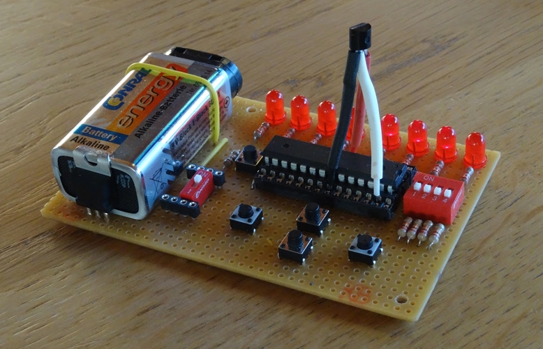
Specifications: 1
ATmega8 microcontroller with TPS firmware, operating at a clock speed
of 4 MHz internal RC oscillator, 256 bytes TPS program storage and 256
bytes log space both in EEPROM Operating voltage: 5V out of a 9V battery pack, stabilized with an L7805 Voltage regulator IC Power consumption: < 4 mA 8 digital output ports able to supply 10 mA each 4 digital input ports with external pulldown resistors and connected to 4 dip switches 4 digital input ports with internal pullup resistors and connected to push buttons 1 reset push button 1 10-bits ADC input 0 - 2.56V 1 10-bits ADC input 0 - 5V 2 PWM outputs shared with 2 programmable 12 chromatical tones audio outputs over 3 octaves
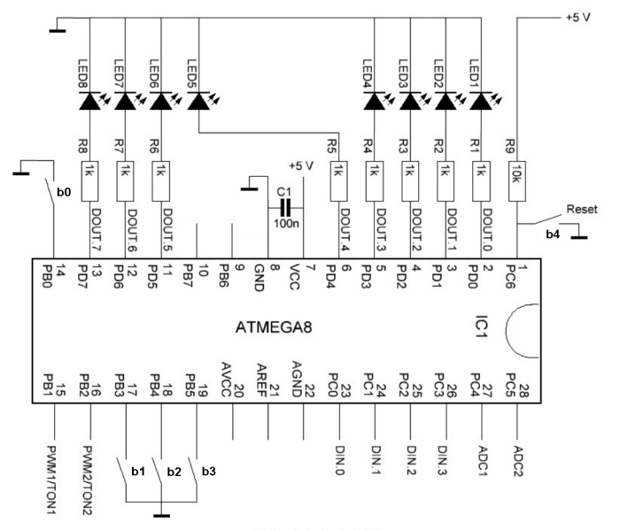
2. Circuit diagram
The
push buttons b0..3 and the LED's 1..8 are used to enter, modify and
debug TPS programs and to retrieve logged data. The LED's can be used
under TPS program control as well; the push buttons too can be called
inside TPS programs to obtain user input.
The digital inputs
DIN.0..3 are specifically meant to be called inside TPS programs. They
are connected to dip switches that can be used to start certain program
fragments. When switched on, they pull the inputs to logical one (+5V).
When off, external resistors pull the inputs to logical zero. In this
situation the inputs can be externally driven. Switches and pulldown
resistors are not drawn.
All
digital input ports are software debounced. The ADC1 input has double
sensitivity compared to the ADC2 input (2.56 and 5V respectively).
Output pins 15 and 16 have double, TPS software controlled functions.
Either they can be configured as PWM outputs or as musical tone
outputs. The reset button b4 resets the controller. Each ATmega8 pin
has a breakout connector, not drawn.
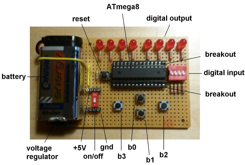
3. Physical layout
The
ATmega8 registers are 1 byte wide. A byte has 8 bits. Therefore, the 8
output LED's can display register contents directly. The LED's are
split into two groups of 4, as one byte is devided in two nibbles of 4
bits. Most instructions are 8 bit sized, so they too can be displayed
as a whole. Instructions that comprise 16 bits, the second part being
data, must be devided over two lines of code and displayed in two
steps. The digital outputs are also available from the breakout strips
to drive other circuits.
The
system is controlled with the four push buttons b0..b3. To give a first
idea: b1 is the Enter-button, whereas b2 and b3 are used to input
nibbles lo and hi respectively. The most important function of b0 is,
in combination with reset, to call the debugger. With b1, in
combination with reset, programming mode is entered. Button b0 also
enables ‘page’ stepping through TPS programs. The four buttons can be
called in TPS programs to receive user input. When not used the buttons
can be externally driven at the breakout strips.
Digital input
to TPS user programs is given with the 4 dip switches. When switched
off, digital input can also be given at the breakout strips.
There
are breakout strips for +5V and ground, and there is an on/off switch.
The voltage regulator stabilizes the 9V battery voltage of to 5V.
See the circuit diagram for more in- and output information. Other details below.
The breakout strips are on a 1:1 basis to the ATmega8 pins. Below a specification of the pins:
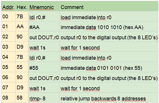
In
these examples Addr. is the address of the instruction, Hex. is the
instruction itself as a hex number, and Mnemonic is the instruction in
a symbolic language more readable than hex code.
“Wechselblinker” program
The
program moves a 10101010 pattern back and forth, slightly different to
the original program, where just one “1” jumps back and forth on the
LED display.
The two mnemonics at addresses 00 and 01 must be
red as one instruction with immediate addressing, the data part of it
being at address 01. The hashtag indicates that there a coupling
between the two bytes. For details on addressing, see above. The data
AA (1010 1010) is loaded into r0. Then, at addresses 02 and 03 the data
is displayed by the LED’s for 1 second. At addr. 04 and 05 the process
is repeated, now with the data 55 (0101 0101). At the end a jump is
carried out to the beginning, so that there is a repeated change in the
LED light pattern (Wechselblinking).
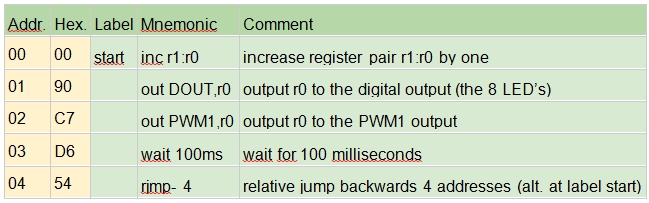
“Binairy counter with PWM output” program
The program counts in binairy and modulates the light of an extra LED based on a binairy number.
At
start it is assumes that r0 = 0, which on reset of the controller is
true. In the first instruction at 00 the register pair r1:r0 is
increased by one. For details about register pairs, see above. Then, r0
is output to the LED’s. This program does not output r1. In the third
instruction, r0 is written to the PWM output 1. A LED connected to the
PWM1 output will vary its light intensity depending on the value of r0.
At address 03 the program is suspended for a short periode of 100 ms,
resumed at address 04 and then proceeds to addr. 00 due to the rjmp- 4
instruction. If, because of the repeated inc’s at address 00, all 8
bits of r0 have been set (1111 1111), r0 becomes 0 (0000 0000) again.
The program thus displays the following sequence of binairy numbers:
<0000 0000> < 0000 0001> <0000 0010> < 0000 0011> < 0000 0100> < 0000 0101> etc. to zero
TPS ATmega8 ’classic+’
by Jos van den Enden and Michael Förster
In
januari 2018, work on an 8-bits push button programmable
microcontroller was published as TPS ATmega8 ‘assembler style’. The
preceding version, developed end 2017, was never published. It was a
first attempt to port work by Burkhard Kainka on a “Tasten-
Programmierbare Steuerung” (TPS) - access here - to an 8-bits version.
After
the publication of the TPS ‘assembler style’ version (which, from now,
we will call version 2), the authors came into contact with each other.
We both realized that it was worthwile to further develop the earlier
version (which, from now, we will call version 1 or TPS ATmega8
‘classic+’). From then we worked together. Our aim was to stay close to
the work of Kainka, but retaining the 8-bits approach, thereby adding
extra features. We were seeing to it that ‘upward compatibility’ with
Kainka’s work - which we refer to as TPS ‘classic’ - was retained as
well.
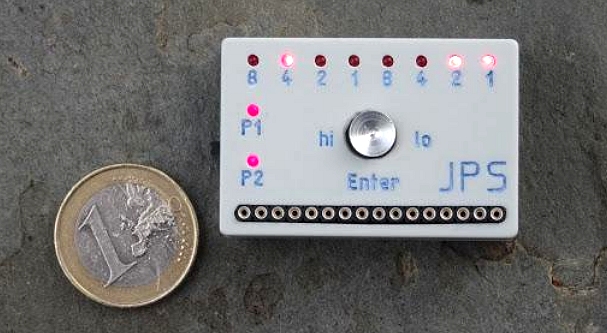
In the manual - access here
- we describe version 1, like version 2 using an ATmega8, firmware
programmed in assembler. A small case was made in which a mini joystick
was used to operate the system (Joystick Programmierbare Steuerung -
JPS!).
As for version 2, a ‘programming aid’ spreadsheet was developed - access here
Below a summary of the most important additions to TPS ‘classic’: - 8-bits mode by default (4-bits mode as an option to retain full upward compatibility) - 8-bits digital outputs to LEDs and breakout connector - 4-directions joystick or 4 push button user inputs - 2 ADC multiple resolution inputs, and 2 PWM multiple resolution outputs - dual channel sound output - more program and data storage memory - user-defined number of constants and variables - subroutine calls up to ten levels deep